Physical Address
304 North Cardinal St.
Dorchester Center, MA 02124
Physical Address
304 North Cardinal St.
Dorchester Center, MA 02124
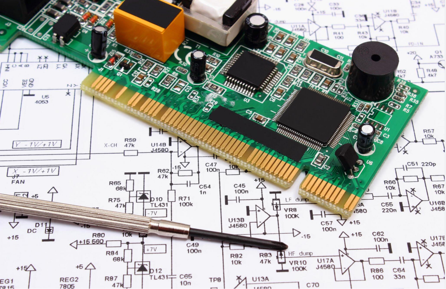
Printed circuit boards, commonly known as PCBs, are the foundation of nearly every electronic device used today. From smartphones and laptops to industrial automation systems, medical equipment, and aerospace electronics, PCBs provide the physical platform that connects and supports electronic components. Without them, modern electronics simply would not exist.
This educational guide explains PCB technology from the ground up. It covers how PCBs work, their structure, manufacturing processes, different types, and why they are essential to modern electronics. The goal is to provide a clear and trustworthy explanation that aligns with industry knowledge and practical engineering principles.
A printed circuit board (PCB) is a flat board made of insulating material that mechanically supports and electrically connects electronic components using conductive pathways etched from copper sheets.
These conductive pathways, often called traces, replace traditional wiring. Instead of manually soldering wires between components, a PCB allows engineers to design precise electrical pathways directly on the board.
A typical PCB serves three main functions:
Because of these functions, PCBs are essential for ensuring stability, reliability, and miniaturization in electronic systems.
Although PCBs can vary widely in complexity, most share a similar structural design consisting of multiple layers.
The substrate forms the rigid base of the PCB. The most commonly used material is FR-4, a fiberglass-reinforced epoxy laminate that provides strength, insulation, and heat resistance.
Other substrate materials include:
Copper foil is laminated onto the substrate and etched to form conductive traces. These traces act like wires, carrying electrical signals between components.
The thickness of the copper layer is measured in ounces per square foot. Common thicknesses include:
The solder mask is the colored coating—usually green—applied over the copper traces. Its purpose is to:
Other solder mask colors include red, blue, black, white, and yellow.
The silkscreen layer contains printed labels and component indicators. It helps engineers and technicians identify component locations during assembly and troubleshooting.
PCBs are classified based on their structure and application. Understanding these types helps engineers choose the right design for specific electronic products.
Single-sided PCBs contain only one copper layer. Components are mounted on one side, and conductive traces run on the other.
Advantages include:
These boards are commonly used in simple electronics such as calculators, toys, and basic household appliances.
Double-sided PCBs contain copper layers on both sides of the board. Components can be mounted on either side, and electrical connections are made through vias—small holes plated with copper.
Benefits include:
Double-sided boards are widely used in consumer electronics and power supplies.
Multilayer PCBs contain three or more copper layers stacked together with insulating material between them.
High-end electronics such as smartphones, servers, networking equipment, and medical devices rely on multilayer PCBs.
Advantages include:
Some advanced PCBs used in telecommunications and computing may contain 10–20 layers or more.
Flexible PCBs are made using flexible plastic substrates that allow the board to bend without breaking.
These boards are commonly used in:
Flex PCBs reduce weight and save space while improving durability in dynamic environments.
Rigid-flex PCBs combine rigid boards and flexible circuits into a single structure. This design is often used in aerospace and military electronics where reliability and space efficiency are critical.
PCB manufacturing involves a series of precise engineering steps that transform raw materials into functional electronic platforms.
The process begins with electronic engineers designing the PCB layout using specialized software such as:
The layout determines the placement of components and routing of electrical traces.
Design files are exported in Gerber format, which acts as the blueprint for PCB fabrication.
Once the design is finalized, the circuit pattern is transferred onto a copper-clad laminate using a photolithography process.
A photoresist layer is applied to the board and exposed to ultraviolet light through a film containing the circuit design.
The exposed areas harden while unexposed sections are removed.
After the photoresist process, chemical etching removes excess copper, leaving only the desired conductive traces.
This step forms the electrical pathways that connect components across the board.
Automated drilling machines create thousands of tiny holes in the PCB.
These holes serve several purposes:
High-end PCBs may use laser drilling to produce microvias for high-density circuits.
After drilling, the holes are plated with copper to create electrical connections between layers.
Electroplating ensures conductivity throughout the PCB stack.
A protective solder mask layer is applied to shield copper traces and prevent accidental solder bridges.
This is the stage where the board gains its recognizable color.
Labels, logos, and component identifiers are printed onto the board using silkscreen technology.
To prevent oxidation and ensure reliable soldering, the exposed copper pads receive a surface finish such as:
Each finish provides different performance characteristics depending on the application.
Before shipment, PCBs undergo electrical testing to verify connectivity and detect manufacturing defects.
Automated systems ensure that:
PCB quality directly impacts the performance and reliability of electronic devices. Poorly manufactured boards can cause issues such as:
High-quality PCB production requires strict control over:
Professional PCB manufacturers invest heavily in advanced fabrication equipment and testing technologies to ensure consistency.
For companies seeking reliable fabrication and engineering expertise, resources such as www.pcbinq.com provide insight into professional PCB manufacturing capabilities and industry solutions.
Designing an effective PCB requires balancing electrical performance, manufacturability, and cost.
High-speed circuits must minimize signal distortion caused by impedance mismatches and electromagnetic interference.
Engineers address these challenges using techniques such as:
Electronic components generate heat during operation. If heat is not properly dissipated, performance degradation or failure may occur.
Thermal management strategies include:
Stable power delivery is critical in modern electronics. Designers use dedicated power and ground planes to reduce voltage noise and improve reliability.
Design for Manufacturability (DFM) ensures that PCB layouts can be produced efficiently without excessive cost or defects.
Common DFM considerations include:
Working with experienced PCB manufacturers helps optimize designs for both performance and production efficiency. For additional insights into fabrication capabilities and PCB engineering services, visiting https://www.pcbinq.com can provide useful technical references.
PCBs play a crucial role across nearly every technology sector.
Devices such as smartphones, tablets, laptops, and smart home products rely heavily on compact multilayer PCBs.
Modern vehicles contain dozens of PCBs controlling systems like:
Electric vehicles require even more sophisticated power electronics boards.
Life-critical medical equipment demands highly reliable PCB designs with strict quality control.
Applications include:
Aerospace electronics require extreme durability under harsh environmental conditions.
Rigid-flex PCBs and high-reliability materials are commonly used in satellites, radar systems, and avionics.
As electronic devices continue to evolve, PCB technology is advancing rapidly to meet new challenges.
Several trends are shaping the future of PCB development.
HDI PCBs use microvias and extremely fine traces to support smaller and more powerful electronic devices.
New substrate materials are being developed to support higher frequencies, improved heat dissipation, and greater mechanical flexibility.
Future PCBs may embed passive components such as resistors and capacitors directly inside the board layers, saving space and improving performance.
Artificial intelligence and automation are transforming PCB manufacturing by improving defect detection, process optimization, and production efficiency.
Printed circuit boards are the backbone of modern electronics, enabling the compact, powerful, and reliable devices that power today’s digital world. From simple single-layer circuits to complex multilayer designs used in aerospace systems, PCBs represent one of the most critical innovations in electrical engineering.
Understanding how PCBs work—from their structure and manufacturing process to design considerations and applications—helps engineers, students, and technology enthusiasts appreciate the sophisticated infrastructure behind everyday electronics.
As industries continue pushing toward smarter devices, faster communication, and more efficient energy systems, PCB technology will remain at the heart of innovation for decades to come.